

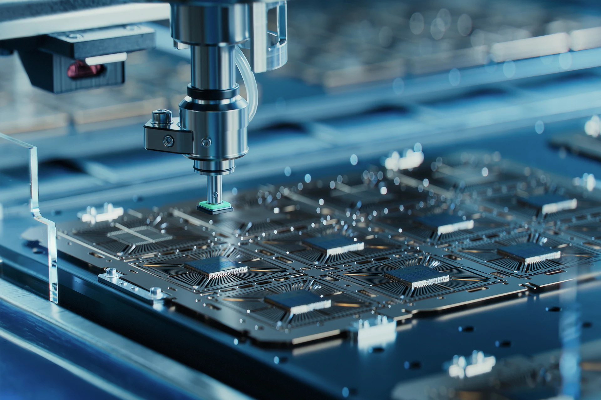
The pace of innovation in the semiconductor industry is increasingly driven by the back end today. Chiplet architectures, 2.5D and 3D packaging, High Bandwidth Memory (HBM), System-in-Package (SiP), and high-performance SiC and GaN semiconductors present new challenges for manufacturing companies. As structure sizes continue to shrink and integration density increases, the requirements for process stability, cleanliness, and long-term reliability are becoming increasingly stringent. Contaminants in the micrometer range or residues from previous process steps can be enough to reduce assembly yield or permanently compromise the reliability of complex semiconductor packages. Cleaning is thus evolving from a downstream manufacturing step to a quality-critical process within modern back-end lines.
The Czech cleaning specialist PBT Works will demonstrate how modern cleaning technologies meet these requirements at SEMICON Taiwan 2026, which will take place in Taipei from September 2 to 4, 2026. As one of the world’s leading trade shows for the semiconductor industry, the event connects manufacturers, material suppliers, and equipment manufacturers, covering the entire semiconductor manufacturing value chain.
Cleaning as part of a controlled process chain
As the complexity of modern semiconductor packages increases, the role of cleaning is also changing. It is no longer limited to the removal of visible contaminants but is evolving into an integral part of qualified manufacturing processes. Reproducible cleaning parameters, documented process data, and controlled cleanliness level play a key role in ensuring stable assembly processes, high yields, and the long-term reliability of modern semiconductor products.
Reproducible cleaning for transfer molding
After Die Attach, Wire Bonding, or Die Bonding or clip bonding, semiconductor devices are often encapsulated using Epoxy Molding Compound (EMC). Depending on the process parameters and subsequent processing steps, residues from assembly process can negatively influence the adhesion of molding compound on the assembly. That can later cause moisture penetration into systems and damage electrical function of the component. PBT Works cleaning systems enable reproducible cleaning processes with precisely controlled process parameters, multi-stage rinsing sequences, and closed media loops. This allows for the creation of clean surface conditions while ensuring high process stability across large production volumes.
Cleaning in Fan-Out Panel-Level Packaging (FOPLP)
As Fan-Out Panel-Level Packaging (FOPLP) continues to gain momentum in high-volume semiconductor manufacturing, the requirements for technical cleanliness throughout the entire process chain are becoming increasingly stringent. Large-format panel substrates pass through multiple process steps, including redistribution layer (RDL) formation, metallization, patterning and molding. Even microscopic particles or contaminants can compromise fine-line structures, reduce process stability or affect the performance of subsequent manufacturing steps. In addition, process carriers, transport fixtures and other manufacturing tooling must be cleaned regularly to prevent particle transfer and cross-contamination within highly automated production environments. Reproducible cleaning processes therefore play an important role in maximizing yield and ensuring stable, high-quality panel-level packaging operations.
Cleaning before underfilling in Flip-Chip Packaging
In Flip-Chip Packaging, surface cleanliness prior to the underfill process is a critical factor for long-term package reliability. Flux residues, ionic and organic contaminants and particulate matter can interfere with the capillary flow of the underfill material, resulting in voids, incomplete filling or delamination between the die and the substrate. Mixing of flux residues with underfill compounds can cause incomplete curing of the material and electrochemical migration. Controlled cleaning before underfill application ensures optimal surface conditions, promotes uniform wetting and supports the formation of reliable interconnects. This contributes directly to the mechanical integrity, thermal performance and long-term reliability of flip-chip assemblies used in advanced semiconductor applications.
Cleaning of power semiconductor packages
Modern power semiconductor packages based on IGBT, SiC and GaN technologies are exposed to high electrical and thermal loads, making process quality and technical cleanliness essential throughout the assembly process. During die attach, soldering or sintering on DCB or AMB substrates, soldering and sintering residues must be removed before subsequent manufacturing steps. Here, cleaning processes with stable and reproducible quality play essential role.
Cleaning of process tools for reliable advanced packaging assembly processes
As modern semiconductor packages become increasingly miniaturized, the requirements for the manufacturing tools used are also rising. Even the slightest deposits on screens, stencils for sinter or flux applications, squeegees, workpiece carriers, or masks can alter the volume of material applied and thus directly affect the quality of subsequent assembly processes. Particularly in fine-pitch applications and during Die Attach of power devices, reproducible paste volumes and homogeneous bondline thickness are key determinants of the package’s long-term reliability. At the same time, residues on workpiece carriers or transport aids can lead to particle carryover and cross-contamination within automated production lines.
PBT Works’ automated cleaning systems ensure that these quality-critical process tools are cleaned in a reproducible and documentable manner. Multi-stage filtration concepts, separate process loops, and continuously monitored cleaning parameters ensure that manufacturing tools can be operated consistently within their specifications, thereby making a significant contribution to the process capability of modern back-end lines.
Cleanliness in the production of high-precision probe cards
Cleaning also plays a crucial role outside of the actual semiconductor assembly process. Modern MEMS, vertical, and cantilever probe cards establish electrical contact between Automatic Test Equipment (ATE) and the bond pads of a semiconductor during wafer testing. Depending on the application, several hundred to several thousand contacts are used simultaneously. The manufacturing of these highly complex test systems involves, among other things, precision assembly, soldering processes, adhesive processes, and Wire Bonding. These processes can leave behind flux residues, particles, or organic contaminants, which can significantly impair the quality of subsequent process steps or negatively affect the long-term electrical performance of the probe cards. A defined level of cleanliness reduces the risk of unacceptable residues on contact structures, and helps ensure the long-term electrical function of these cost-intensive manufacturing tools. Especially for custom probe cards with correspondingly high manufacturing costs, consistent cleaning processes play a key role in reducing rework and scrap.
For these demanding cleaning applications in the semiconductor industry, Asian customers use the SuperSWASH III, for example. Its powerful linear spray system, separate washing and rinsing circuits operated in a closed loop, and reliable hot-air drying enable reproducible cleaning of tools, complex components, and assemblies.
Visit PBT Works at SEMICON Taiwan 2026, TaiNEX 1, stand J2546 and talk with our cleaning experts about how cleaning technologies can be specifically integrated into modern semiconductor back-end and advanced packaging processes.